


Lifetime Achievement Award 2024


The Team that Created the First NAND-type 3D Flash Memory
The team of Hideaki Aochi, Ryota Katsumata, Masaru Kito, Masaru Kido, and Hiroyasu Tanaka of Toshiba, now KIOXIA, created the first 3D NAND Flash.
NAND Flash Reaches the End of Moore's Law Scaling
When Gordon Moore first proposed what became known as Moore's Law in 1965, he plotted the development of memory chips and proposed that an IC with 65,000 devices would appear by 1975, and that the growth of transistors per chip would reduce the cost of a transistor. His prediction has driven the migration of the semiconductor industry to ever-smaller processes, and with it the continued reduced cost of transistors.
However, by the time of its 15nm process node, NAND flash was unable to continue this progression. This was because the shrinking process geometries had created a situation in which the coupling between adjacent flash cells overwhelmed the coupling of any single bit cell to its own control gate. Although earlier inventions had brought cell sizes from their originally-anticipated limit of 45nm down to 15nm, the industry then ran out of techniques to take the technology any further. As such, a new approach was needed.
Moving in a New Direction
When a team of researchers at Toshiba (now KIOXIA*) studied this problem, they reviewed then-current "crosspoint" approaches to stacking memory layers to reduce costs. However, this approach was seen as unable to continue Moore's law scaling for more than a single generation. (*The memory business of Toshiba Corporation was spun off and named as Toshiba Memory Corporation in April 2017, and Toshiba Memory Corporation changed its name to KIOXIA Corporation in October 2019.)
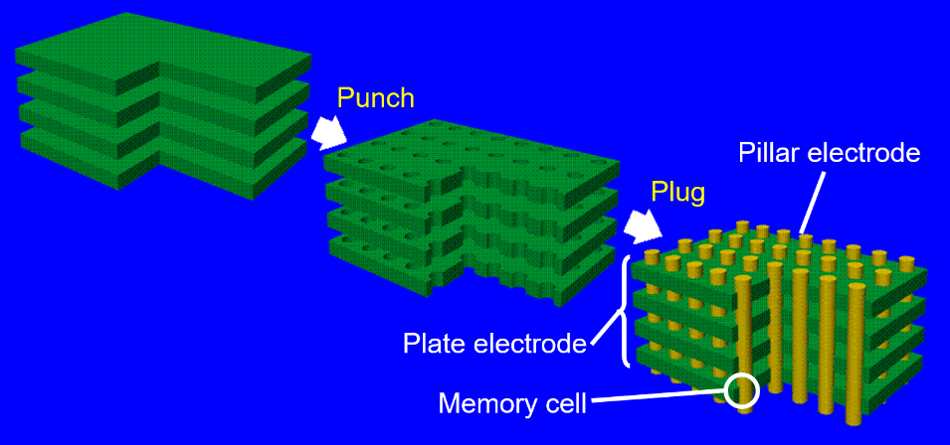
Instead, a new approach was devised by depositing multiple pairs of conductive and insulating layers onto the base wafer. The conductive layers (the green layers in Fig. 1) serve as plate electrodes to act as the control gate for the flash bit cells. After multiple layers have been formed, a large number of holes are etched (punched) perpendicular to the plate electrode surfaces. Each hole is then filled (plugged) with column-shaped electrodes (the "Pillar electrodes" in Fig. 1) and a charge storage film. This process creates memory cells at the intersections of the plate electrodes and the pillar electrodes, as also shown in Fig. 1.
This "Punch & Plug" structure is able to produce multiple layers of NAND-type 3D flash in a single lithographic step, resulting in significant cost savings since lithography is flash memory's most costly process. This approach has allowed scaling to progress by adding layers, rather than shrinking transistors laterally. As a result, since bit costs have continued to scale down to follow Moore's Law, KIOXIA has called it "BiCS FLASH™."
The Success of the BiCS FLASH™ Architecture
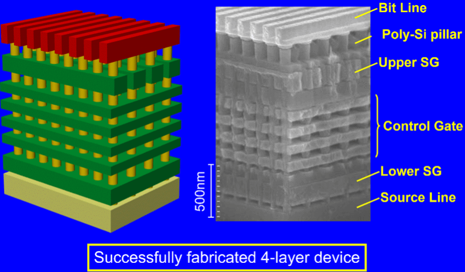
KIOXIA's 3-dimensional (3D) NAND-type Flash Memory technology was first publicly disclosed in 2007 at the IEEE VLSI Symposium. Another important paper on BiCS FLASH™ was presented the following year at the 2008 IEEE IEDM. These papers disclosed how this concept would transform NAND type Flash Memory from its conventional 2D horizontal structure to a 3D vertical structure consisting of a set of layers within a die. BiCS FLASH™ thus overcame the 2D density limit of flash memory through multilayer cell array stacking. Importantly, BiCS FLASH™ allows several layers to be fabricated in a single lithography step. An early prototype is in Fig. 2.
Progression of the BiCS FLASH™ Architecture
While the BiCS FLASH™ design disclosed in the early technical papers described a 4-layer device, the following outlines many of the milestones for this architecture (see also here):
- 2015: Commercialized 48-layer 128 Gbit MLC BiCS FLASH™
- 2015: Commercialized 48-layer 256 Gbit TLC BiCS FLASH™
- 2016: Commercialized 64-layer 256 Gbit TLC BiCS FLASH™
- 2017: Commercialized 64-layer 512 Gbit TLC BiCS FLASH™
- 2017: Announced 96-layer 512 Gbit TLC BiCS FLASH™
- 2020: Announced 112-layer 512 Gbit TLC & QLC BiCS FLASH™
- 2021: Announced 162-layer 1 Tbit TLC BiCS FLASH™ using CMOS Under Array (CUA) placement
- 2023: Announced 218-layer 1 Tbit TLC & QLC BiCS FLASH™ using CMOS directly Bonded to Array (CBA) technology
- 2024: Announced 218-layer 2Tbit QLC BiCS FLASH™ using CBA technology
The dramatic architectural change of going 3D has enabled flash to continue to provide Moore's Law cost reductions.
IEEE's Andrew S. Grove Award
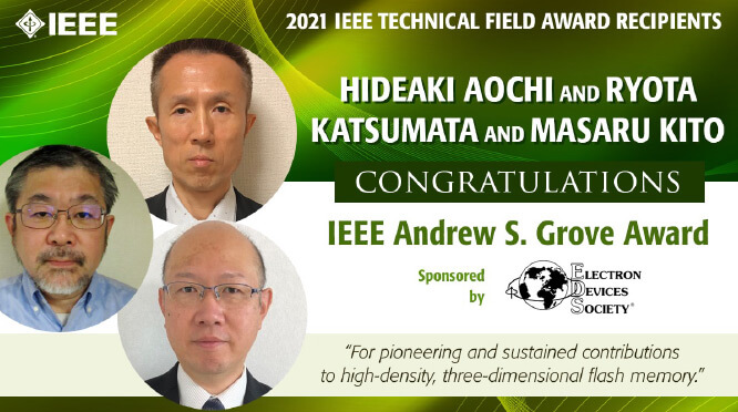
The Andrew S. Grove Award is a Technical Field Award presented by the IEEE for outstanding contributions to solid-state devices and technology. In 2021, three of the BiCS FLASH™ technology inventors received this prestigious award on behalf of the team "for pioneering and sustained contributions to high-density, three-dimensional flash memory" from the IEEE Electron Devices Society (EDS). See Fig. 3. Stefan Lai, 2011 FMS Lifetime Achievement Awardee, received this award in 2008.
Japan's Imperial Invention Prize
The 2020 Imperial Invention Prize from the National Commendation for Invention was awarded to the KIOXIA BiCS FLASH™ team for the 3D Flash Memory Device and Manufacturing Method (as described in Japanese Patent No. 5,016,832) for a method to greatly increase memory capacity and decrease manufacturing costs. The prize recipients were Masaru Kito, Hideaki Aochi, Ryota Katsumata, Masaru Kido, Hiroyasu Tanaka, and Akihiro Nitayama. This prize's Implementation Achievement Awardee was KIOXIA President and CEO Nobuo Hayasaka. See also here.
Japan's Award for Science and Technology
The 2023 Award for Science and Technology from Japan's Ministry of Education, Culture, Sports, Science and Technology was awarded to the KIOXIA BiCS FLASH™ team for their invention of high-density 3D flash memory, and its manufacturing method. The awardees were Ryota Katsumata, Masaru Kito, Hideaki Aochi, Masaru Kido, and Hiroyasu Tanaka. See also here.